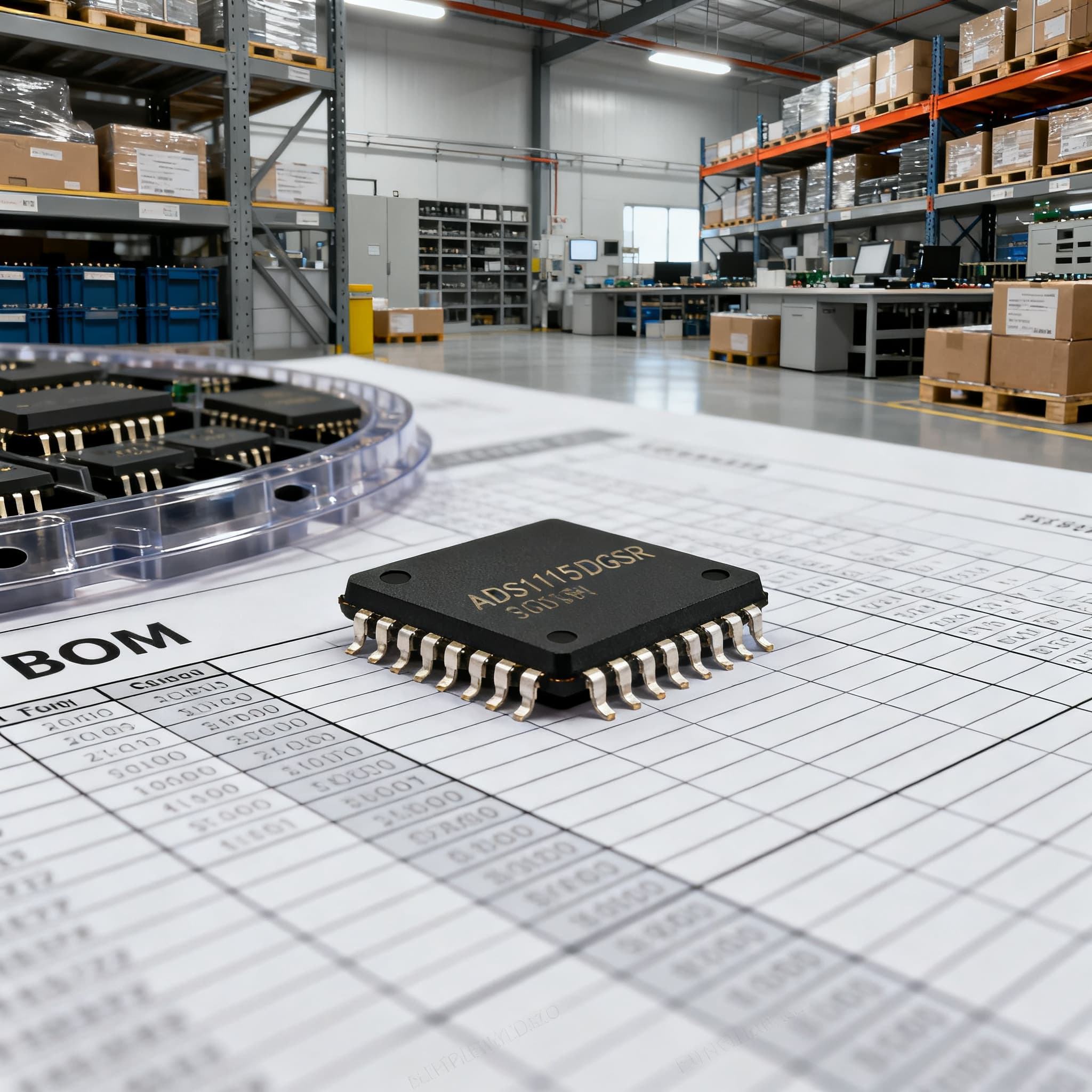
ADS1115IDGSR Procurement Guide: Pinout and Spec Checks for RFQ
ADS1115 procurement checklist: datasheet specs and pinout fields to verify on RFQ, plus BOM upload path on BOMNow.
When 'Active' Isn't Enough: The ADS1115 Lifecycle Signal That Alters Procurement Deadlines
You pull a BOM line item forADS1115IDGSR and the distributor portal flashes green — "Active." For many procurement managers, that is where the check ends. The Texas Instruments ADS1115 family has been shipping for over a decade, and the ADS1115 in its VSSOP‑10 variant still appears on thousands of approved vendor lists. But "Active" and "safe to specify for a 2027 production ramp" are two very different things for a mature 16‑bit delta‑sigma ADC.
The term you actually need to watch for is NRND — Not Recommended for New Designs. As the team at PCNshark explains, NRND means "the part is still produced and orderable, but the manufacturer advises against using it in new designs." No formal end‑of‑life date has been published, but the yellow banner on the product page changes everything. Once NRND status appears, the window can last anywhere from one to many years, but supply availability becomes progressively less reliable and more expensive, as Industrial Monitor Direct's engineering guide underscores: "Final shipment dates and order cutoffs are explicitly specified in the formal PCN. For new designs, never select an NRND component."
Procurement takeaway: Before locking a 12‑month PO for ADS1115IDGSR, pull TI's product lifecycle page and check for any PCN issued in the preceding 18 months. The TT Electronics lifecycle application note recommends reviewing lifecycle status at least annually with a maximum horizon of five years. For a part this mature, an unexpected NRND flag can compress your last‑time‑buy window to weeks. Independent verification through lifecycle tracking tools is not overkill — it is baseline due diligence when a single ADC line item gates an entire sensor‑front‑end PCBA shipment.
ADS1115IDGSR Pinout Decoded: VSSOP‑10 Connections, PGA Setup, and the I2C Address Pin Reality
TheADS1115IDGSR ships in a 10‑pin VSSOP (MSOP‑10) package whose compact footprint hides several sourcing traps. If your PCB layout was drawn from a generic ADS1115 block diagram rather than the exact TI datasheet (SBAS444E, also mirrored by Adafruit), you may have missed critical pin‑function details that affect both procurement and integration.
The pin assignment per the AllDatasheet entry and the Fly‑Wing pinout guide is straightforward at first glance:
- AIN0–AIN3 (pins 4–7): Four single‑ended or two differential analog inputs. Single‑supply only — the ADS1115 cannot accept negative voltages relative to GND.
- VDD (pin 10) and GND (pin 3): Supply range 2.0 V to 5.5 V.
- SDA (pin 9) and SCL (pin 8): Standard I²C lines with pull‑up resistors required externally.
- ADDR (pin 1): Sets the I²C slave address. This is the single most‑misconfigured pin in multi‑ADC designs.
- ALERT/RDY (pin 2): Programmable comparator output or conversion‑ready indicator. Open‑drain; needs a pull‑up.
ADS1115IDGSR more than a commodity ADC for sensor procurement. The internal 2.048 V reference, combined with PGA gain settings, defines the full‑scale range per channel. Getting this wrong at the RFQ stage — for instance, specifying a gain that clips your sensor output — leads to respins disguised as sourcing problems.
| PGA Gain Setting | Full‑Scale Range (FSR) | LSB Size | Typical Sensor Match |
|---|---|---|---|
| ⅔ (±4.096 V) | ±4.096 V * (2/3) ≈ ±2.733 V | 83.3 µV | Limited use; verify input common‑mode |
| 1 (±4.096 V) | ±4.096 V | 125 µV | 0–5 V industrial sensors, 4–20 mA shunt |
| 2 (±2.048 V) | ±2.048 V | 62.5 µV | 3.3 V ratiometric bridge sensors |
| 4 (±1.024 V) | ±1.024 V | 31.25 µV | Low‑output load cells, thermocouple amps |
| 8 (±0.512 V) | ±0.512 V | 15.625 µV | Precision strain gauges, microvolt signals |
| 16 (±0.256 V) | ±0.256 V | 7.8125 µV | High‑gain sensor front‑ends; noise‑limited |
Tip: The PGA gain table is not academic. If your sourcing team receives an RFQ with "ADS1115IDGSR, qty 5k," but the end application is a 3.3 V‑supplied wheatstone bridge producing ±1.5 V differential output, gain = 2 (FSR ±2.048 V) is the correct starting point. Gain = 1 would waste nearly half the ADC codes. Gain = 4 would saturate. That mismatch — caught only after production — burns both the ADC inventory and the assembly run.
The ADDR pin deserves a standalone warning. The datasheet specifies four I²C addresses by connecting ADDR to GND (0x48), VDD (0x49), SDA (0x4A), or SCL (0x4B). FourADS1115IDGSR devices can coexist on one bus without a multiplexer, but only if the board layout ties ADDR correctly. A floating ADDR pin yields an indeterminate address and intermittent bus failures — a classic field‑return driver that looks like a counterfeit part but is actually a design‑side oversight.
ADS1115IDGSR vs. ADS1115-Q1 and Other 16‑Bit ADC Choices: Mapping the BOM Trade‑Offs
When a distributor reports 26‑week lead time onADS1115IDGSR, the instinct is to search for a fast substitute. Two candidates routinely surface: the ADS1115‑Q1 (TI's automotive‑qualified sibling) and the MCP3421 from Microchip, which Components101 lists as a functional alternative in the same 16‑bit delta‑sigma class. But "functional alternative" and "drop‑in BOM replacement" are separated by package, temperature grade, and qualification requirements — and procurement owns the verification burden.
| Comparison Metric | ADS1115IDGSR (Commercial) | ADS1115‑Q1 (Automotive) | MCP3421 (Microchip) | Selection Criteria & Failure Boundary |
|---|---|---|---|---|
| Package | VSSOP‑10 (3.0 × 3.0 mm) | VSSOP‑10 or UQFN‑10 | SOT‑23‑6, DFN‑6 | UQFN‑10 is not footprint‑compatible with VSSOP‑10; verify before swapping |
| Operating Temp. | −40°C to +125°C | −40°C to +125°C (AEC‑Q100) | −40°C to +125°C | Q1 adds AEC‑Q100 qualification; non‑automotive designs pay a premium for unneeded certs |
| Channels | 4 single‑ended / 2 differential | 4 single‑ended / 2 differential | 1 single‑ended / 1 differential | MCP3421 is single‑channel; multi‑sensor BOMs need layout and firmware rework |
| PGA | Yes, 6 gain steps (⅔ to 16) | Yes, same PGA range | Yes, 3 gain steps (1, 2, 4, 8) | Fewer gain options in MCP3421 may require external amplification for some sensors |
| Internal Reference | 2.048 V | 2.048 V | 2.048 V | All three use internal reference; no external VREF procurement needed |
| I²C Addresses | 4 (0x48–0x4B) | 4 (0x48–0x4B) | 8 (0x68–0x6F) — fixed | MCP3421 offers more bus addresses but fewer channels; trade channel count for density |
| Max Data Rate | 860 SPS | 860 SPS | 240 SPS (at 16‑bit) | ADS111x is 3.6× faster; MCP3421 may miss transient events in fast control loops |
| Qualification | Commercial | AEC‑Q100 Grade 1 | Commercial | Q1 is for automotive; commercial designs over‑specifying Q1 inflate BOM cost 15–30% |
| ESD Rating | 2 kV HBM (typical) | 2 kV HBM, higher CDM | 4 kV HBM | MCP3421 leads on HBM; relevant for harsh‑environment sensor nodes |
The ADS1115‑Q1 warrants separate scrutiny. Functionally, the register map and I²C command set are identical to the commercial ADS1115IDGSR. But TI's ADS1115‑Q1 product page confirms it ships in a UQFN‑10 option that shares no footprint with the VSSOP‑10. "Drop‑in" is a dangerous word here. If your assembly house has stencils and pick‑and‑place programs built around the VSSOP‑10, switching to UQFN‑10 requires a full SMT process requalification — tape‑and‑reel orientation, thermal profile, and AOI inspection parameters all change.
ADS1115IDGSR analog inputs means replicating four MCP3421 chips plus an I²C bus re‑design. The BOM line count grows, and the cost advantage evaporates. Reserve that comparison for new designs, not for shortage‑driven VSSOP‑10 replacement orders.
Why Precision Sensor Front‑Ends Rely on ADS1115IDGSR: From Bridge Sensors to Low‑Side Current Shunts
Understanding where theADS1115IDGSR sits in the end application sharpens your RFQ specifications. Three application patterns dominate procurement for this part, and each carries distinct verification requirements.
1. Wheatstone Bridge Load Cells and Pressure Sensors. A full‑bridge strain gauge excited at 3.3 V typically outputs ±15 mV to ±30 mV differential across its sense nodes. With the ADS1115IDGSR's PGA set to gain = 128 (on‑chip, though the table above covers the standard six settings; verify extended gain availability in the latest datasheet revision), the full‑scale range drops to approximately ±0.256 V, yielding 15.6 µV per LSB — enough to resolve a 1 kg load cell to better than 0.1% without an external instrumentation amplifier. This is the exact use case the Fly‑Wing sensor interfacing guide walks through, noting that the ESP32's built‑in ADC exhibits well‑documented non‑linearity and drift, which is why precision projects replace it with an external ADS1115IDGSR. From a procurement perspective, the PGA eliminates two external op‑amps, four precision resistors, and a voltage reference — collapsing six line items into one.
2. 4–20 mA Loop Monitoring. A precision shunt resistor (typically 100 Ω to 250 Ω) in the return path converts 4–20 mA to 0.4–5.0 V. The ADS1115IDGSR, with PGA gain = 1 and FSR = ±4.096 V powered from a 5 V rail, digitizes the entire loop range with margin. The internal 2.048 V reference means no external voltage reference needs sourcing, qualification, or traceability paperwork.
3. Low‑Side Current Measurement. The Adafruit‑hosted datasheet includes Figure 38, explicitly showing a low‑side current shunt configuration where the ADS1115IDGSR measures the voltage drop across a sense resistor placed between the load and ground. This topology appears in motor driver feedback loops, battery fuel gauging, and solar charge controllers. The caution in the datasheet is unambiguous: the ADS1115 can only accept positive voltages. Any negative excursion on the shunt — even a transient — violates the input range and can cause incremental damage leading to "slow, long‑term failure." For procurement, this reinforces the importance of confirming the end application's voltage swing before committing to volume orders. A design that works on the bench with a clean lab supply may fail in the field with a noisy motor load.
Across all three patterns, the common thread is the TI ADS1115 product page specification: a single‑chip analog front‑end that replaces discrete signal‑conditioning chains. That consolidation reduces BOM line count, simplifies supplier management, and lowers assembly cost — provided the PGA gain range and input common‑mode constraints are respected at the design‑verification stage, not discovered during incoming inspection.
Pre‑RFQ Pin‑Level Due Diligence: Spotting Address Pin Traps, Voltage Range Blunders, and Package Variant Errors
A well‑constructed RFQ forADS1115IDGSR does not start with quantity and target price. It starts with a five‑minute datasheet cross‑check that prevents the three most expensive procurement errors. The following actionable checklist is built from field observations across sensor‑module, industrial I/O, and metering BOMs.
- Verify the full ordering code: ADS1115IDGSR, not ADS1115IRUGR or ADS1115BQDGSRQ1. The "IDGSR" suffix denotes the VSSOP‑10 package, tape‑and‑reel (2500 units), commercial temperature grade. Confusing it with the "IRUGR" (X2QFN‑10) or "BQD" (QFN) suffix yields physically incompatible parts. The TI product page lists every active ordering code; cross‑reference your internal BOM against the manufacturer's OPN (Orderable Part Number) list before hitting "send" on the RFQ.
- Confirm input common‑mode range: 0 to VDD. The ADS1115IDGSR cannot digitize signals below GND. If the sensor front‑end produces bipolar outputs (±2.5 V), a level‑shift circuit must precede the ADC. No amount of PGA gain adjustment fixes a negative input — the ADC simply clips or, worse, degrades over time, as the datasheet's incremental‑damage warning cautions.
- Audit the ADDR pin strapping on the PCB. If your design uses two or more ADS1115IDGSR devices on the same I²C bus, each ADDR pin must be tied to a unique rail (GND, VDD, SDA, SCL). A floating or mis‑strapped ADDR pin creates bus contention that mimics a batch‑wide component failure. Before attributing field failures to "counterfeit ADCs," have the engineering team verify address‑pin voltages with an oscilloscope — the fix may be a single resistor change, not a supplier change.
- Check TI's PCN history and lifecycle status within 90 days of RFQ submission. The PCNshark lifecycle resource and the TT Electronics lifecycle tracking application note both emphasize that NRND status can appear with minimal warning. Set a calendar reminder to re‑verify lifecycle status quarterly if the ADS1115IDGSR anchors a production BOM with a planned run of 18 months or longer.
- Specify date code and traceability requirements in the RFQ. For high‑reliability sensor front‑ends — medical instrumentation, precision metering, industrial safety loops — request full lot traceability back to TI's assembly site. Open‑market sources may offer lower pricing but cannot always guarantee a single date‑code batch. Mixed date codes across a production run can create subtle performance variations that are nearly impossible to diagnose after deployment.
Key takeaway: The ADS1115IDGSR is not a commodity resistor network. It combines a precision voltage reference, a programmable‑gain delta‑sigma modulator, and an I²C digital interface in a 3 mm‑square package. Treating its procurement as a simple PN‑to‑PN match — without verifying the pin‑level and lifecycle details above — is the shortest path to a line‑down situation that no expedited shipment can fix.
| Pre‑RFQ Action | When to Use | Trade‑Off / Risk If Skipped |
|---|---|---|
| Cross‑check OPN suffix against TI.com ordering codes | Every RFQ; especially when BOM inherited from a legacy design | Wrong package lands on SMT line; rework costs exceed ADC unit savings |
| Verify ADDR pin strapping for multi‑ADC designs | Designs with ≥2 ADS1115IDGSR on one I²C bus | Indeterminate bus addresses; intermittent failures; field returns |
| Confirm input voltage polarity vs. sensor output | New sensor integration or replacement sensor with different output stage | ADC clipping or long‑term damage; datasheet warns of incremental failure |
| Review TI PCN history and lifecycle status | Quarterly for active production BOMs; within 7 days of large‑volume RFQ | NRND or EOL surprises compress last‑time‑buy window; allocation risk |
| Request single date‑code lots with traceability docs | Medical, metering, safety‑critical, and Class‑2 industrial applications | Potential batch‑to‑batch offset variation; calibration drift post‑deployment |
| Bench‑test a sample batch before committing to 10k+ volumes | First article inspection or supplier re‑qualification | Undetected marginal parts propagate across production build; recall exposure |
Quick‑Fire Questions on ADS1115IDGSR Sourcing and Integration
Q: Does the ADS1115IDGSR require an external voltage reference?
No. The ADS1115IDGSR integrates a 2.048 V internal voltage reference, which is factory‑trimmed and temperature‑compensated. The full‑scale range at the default PGA gain of 1 is ±4.096 V. You do not need to source, qualify, or stock a separate precision reference chip — one of the primary reasons this ADC reduces BOM line count in sensor front‑end designs. However, if your system accuracy budget demands better than the internal reference's drift specification over temperature, verify the datasheet's typical and maximum drift curves on the TI ADS1115 product page.
Q: How many ADS1115IDGSR devices can share a single I2C bus without a multiplexer?
Four. By tying the ADDR pin to GND (address 0x48), VDD (0x49), SDA (0x4A), or SCL (0x4B), you set four unique slave addresses on the same I²C bus. This is verified across the SBAS444E datasheet and the Fly‑Wing pinout guide. Beyond four devices, an I²C multiplexer or separate bus segment is required. For procurement, confirm with engineering whether the design uses all four address slots — if not, there is expansion headroom without adding a mux to the BOM.
Q: What is the primary supply risk for the ADS1115IDGSR given its mature status?
An unexpected NRND or EOL notification from Texas Instruments. Although the ADS1115IDGSR is currently orderable through authorized distribution, its maturity means a lifecycle change can arrive with limited advance warning. As FPGACenter's IC lifecycle guide notes, NRND can last from one to many years with no fixed timeline. The TT Electronics lifecycle note recommends independent tracking beyond what a single distributor portal displays. Before submitting any RFQ above prototype volumes, check TI's product page lifecycle field, review recent PCNs, and consider a second‑source verification through a dedicated lifecycle monitoring service.
Q: Is the ADS1115-Q1 a straightforward drop‑in replacement for the ADS1115IDGSR?
No. While the ADS1115‑Q1 shares the same register map, I²C command set, and internal PGA/reference architecture, the ADS1115‑Q1 product page confirms it is offered in VSSOP‑10 and UQFN‑10 packages. The UQFN‑10 variant does not share a footprint with the VSSOP‑10 used by the ADS1115IDGSR. Additionally, the Q1 suffix brings AEC‑Q100 qualification and an extended temperature range specification that may not be necessary for commercial or industrial designs. Substitution requires a full fit‑form‑function review: verify package, temperature grade, ESD tolerance, and assembly process compatibility. Do not assume a same‑family Q1 part lands on your existing PCB pads.
References & Further Reading
- Texas Instruments — ADS1115 Product Page, Datasheet, and Ordering Information
- Texas Instruments — ADS1115‑Q1 Automotive‑Grade Product Page
- Adafruit — ADS1115 Datasheet SBAS444E (Mirror)
- AllDatasheet — ADS1115 Datasheet Quick Reference
- Fly‑Wing — ADS1115 Pinout, PGA Configuration, and Sensor Interfacing Guide
- Components101 — ADS1115 Module Overview with Alternatives
- PCNshark — Electronic Component Lifecycle Status: Active, NRND, EOL, and Obsolete
- FPGACenter — EOL vs. NRND vs. Obsolete: IC Lifecycle Status Explained
- Industrial Monitor Direct — Understanding NRND Component Status
- TT Electronics — Instant Access to Life Cycle and Obsolete Product Data (Application Note TN007)
The ADS1115IDGSR delivers exceptional front‑end consolidation for sensor‑interface BOMs — four differential channels, six PGA gain steps, and an internal voltage reference in a 3 mm‑square VSSOP‑10 — but its procurement demands more than a simple PN match. Address‑pin strapping errors, package‑suffix confusion, and overlooked lifecycle signals have stranded more production lines than genuine silicon shortages ever did. Treat every RFQ for this part as an opportunity to re‑verify: pull the latest TI datasheet revision, confirm the ADDR pin plan, check for PCNs, and specify traceability appropriate to your application's reliability tier. When you are ready to consolidate that due diligence into a single sourcing action, Upload Your BOM for a consolidated quote